Mind the BandGap — It's Gotten Wider!
New Wide Bandgap Technologies in Next-Generation Power System Designs

Image Source:
MJgraphics/shutterstock.com
By Paul Lee for Mouser Electronics
Published March 6, 2020
The Burning Issue: Minimizing Heat Generation
Global electrical energy demand is now at a staggering level—with nearly 30 petawatts forecast in 2020, according
to the International Energy Agency. This is an almost incomprehensible number to those of us who can only
appreciate high power in multiples of 1kW toasters. The figure is set to increase, driven mainly by Asian
economies, and, of course, a focus is to meet the demand from renewable sources in order to mitigate climate
change effects. Intercepting solar, wind, and other green energy sources to extract electricity before it is
converted to heat should have no net warming effect, but while fossil fuels are still a major source of energy,
heat is released that would otherwise remain "locked up." The efficiency of the conversion process from raw
mineral to useful work is therefore critical to avoid yet more excess energy being lost to the
environment—and to save costs.
Today, the main use of energy is in industrial processes, particularly driving motors. But data centers aren't
far behind, and demand from electric vehicle (EV) charging is set to explode in the years ahead. These
applications, along with many others, from home appliances to phone chargers, have all seen technology
innovations to minimize power draw, typically using "smart" techniques such as variable-frequency drives for
motors. This entails using electronic power supplies, and the spotlight is now firmly on them to show ever lower
conversion losses. Here, we will look at how designers now have access to semiconductor switch technologies that
make highly efficient power converters easier to realize.
Power Conversion Challenges and Topologies
We all say "power converters," but this is a bit of a misnomer—the ideal is to achieve exactly the same
power output from the device as is input. This is what power converter designers strive for: To convert
electrical energy from a distribution system, typically AC mains or a DC bus, to a different DC or sometimes AC
voltage, all without dissipating power as waste heat. Sometimes galvanic isolation is necessary through
transformer coupling, for safety or functional reasons; the output voltage can be higher or lower than the
input, actively regulated or not, but in all cases the "switched mode" technique has become ubiquitous.
For years, bi-polar semiconductors have been the conventional choice where electrically controllable switches
were needed, such as in power conversion and motor drive applications. But that trend has seen changes, first to
metal-oxide-semiconductor field-effect transistors (MOSFETs), and now to Gallium Nitride (GaN) and Silicon
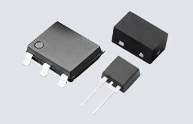
Carbide (SiC) devices. Both GaN and SiC devices, such as insulated-gate bipolar transistors (IGBTs) with their
optimal thermal performance and high switching capabilities, are ideal for high-voltage and high-power switching
applications (Figure 1).
Figure 1: The high-switching capabilities and excellent thermal performance
of SiC and GaN devices make them ideal for use in high-voltage and high-power switching applications.
(Source: Forrest9/shutterstock.com)
Topologies of converters have also been refined, with the most efficient being "resonant" types in multi-switch
half- or full-bridge configurations at high power. Three-phase bridges using IGBTs or MOSFETs are now commonly
used to produce AC for motor drives. In all these topologies, ideal switches dissipate no power when they are
off or on, and ideal inductors, transformers or capacitors dissipate no heat, so the focus of converter design
is to use components that are closest to the ideal in performance while minimizing any transient dissipative
conditions, such as when switches slew between on and off states. In modern designs, these "switching" losses
are the largest contributors and can have high peak values.
Losses are clearly proportional to the number of switching transitions per second (frequency), so for the
semiconductors, low frequency is better. Core losses in magnetic components are also higher as frequency
increases, but their size, weight, and cost reduce, along with copper losses, so the frequency chosen is a
compromise and can vary from a few kHz in motor drives to several MHz when size is a priority, for example in
telecom applications.
The latest SiC and GaN wide bandgap devices have inherent switching speeds so fast that it would be a challenge
to measure their values; however, parasitic capacitances internal to and around the devices slow speeds to the
nanosecond range. Device output capacitance, COSS, and the energy required to charge and discharge
it, EOSS, are therefore important figures-of-merit (FOM), along with on-resistance RDS(ON)
for MOSFETs, which can be critical at high currents. The product of on-resistance and die area,
RDS(ON)• A is another important FOM of total losses, because capacitances and their associated
switching losses reduce as die area shrinks.
Wide Bandgap Semiconductors Explained
Let's explain what we mean by "wide bandgap" (WBG) devices. These are SiC and GaN semiconductors, which require
relatively high energy to move electrons from their atomic "valence" band to its "conduction" band, where they
are available for current flow. The "bandgap" is measured in electron-volts (eV), with the value for silicon
(Si) being about 1.1eV, while SiC is 3.2eV, and GaN is 3.4eV. High bandgap values give higher critical breakdown
voltages and lower leakage currents, especially at high temperatures. Moreover, WBG devices also have better
electron saturation velocity, leading to faster switching. SiC devices also tend to exhibit superior thermal
conductivity.
We know that smaller die size reduces WBG device capacitances and enables faster switching. Another result of
smaller die size is significantly reduced gate-drive power requirements. Traditional technologies in silicon for
MOSFETs and IGBTs in particular have yielded high values for gate charge required for efficient switching,
sometimes in the order of microcoulombs for IGBTs and hundreds of nanocoulombs for power MOSFETs (Figure
2). This has required significant drive power, in the order of watts for the larger IGBTs,
contributing significantly to system losses. For WBG devices, the figure can be just milliwatts, even at high
frequencies.
Figure 2: Power MOSFET losses can be affected by their size. (Source:
science photo/shutterstock.com)
There are yet more WBG device benefits. For example, they are inherently able to operate at much higher
temperatures than silicon, with some manufacturers showing their devices working at peaks of over 500°C.
Although packaging practically limits temperatures to lower operating values, the high peak capability gives
confidence in robustness under transient stress conditions. Variation with temperature of critical values such
as gate leakage and on-resistance is also much lower compared with silicon, and the wide bandgap even makes the
devices much more radiation-resistant for hi-reliability applications in aerospace.
WBG Device Developments
The case for using WBG devices is compelling when the potential performance comparisons are made with IGBTs and
Si-MOSFETs, although these devices still dominate the market for power switching and are themselves being
improved with new generations. Being new technology, WBG costs have initially been higher than silicon but
prices are lowering, and knock-on system benefits offset this to a large extent. For example, significant
improvements in efficiency are possible, along with corresponding reduction in size, weight, and therefore cost
of other components, such as heatsinking, and inductors and capacitors used in output and EMC filtering. System
functional performance can also improve with faster switching speeds, with quicker response to load changes and
smoother control of motors, for example.
WBG Device Manufacturers
WBG device manufacturers can make the case that, overall, the value of using their devices is such that they
should be considered for any new applications in power conversion, and they have put much effort into refining
the technologies so that the parts are easy to use and robust, particularly under fault conditions such as
short-circuits and over-voltages that are common in motor drives (Figure 3).
Figure 3: New manufactured devices are easy to use and robust. (Source:
asharkyu/shutterstock.com)
Let's take a look at some of the WBG device manufacturers and how they incorporate WBG technology into their
products.
Infineon
Infineon, for example,
demonstrates the reliability of its SiC MOSFET gate oxide interface, which could fail if it had defects, or at
least reduce channel mobility and on-resistance. As a solution, it has chosen a trench construction, which
enables a low channel resistance at low gate electric field strengths. GaN High Electron Mobility Transistor
(HEMT) devices from Infineon use a planar construction. Unlike SiC MOSFETs, HEMTs have no body diodes, making
them particularly suitable for "hard switching" applications. The construction is designed to work in
enhancement mode as with SiC MOSFETs, but unlike them, there is no gate insulation, so a small gate current is
required to keep the devices turned on.
On-state gate threshold voltage is also low, typically around 1.4V. GaN devices are offered with ratings at 600V
compared with 1200V and higher for SiC, but the theoretical limit for GaN RDS(ON) at a particular voltage rating
is about 10 times better than SiC.
STMicroelectronics
STMicroelectronics claims the highest temperature rating in the industry, at 200°C
for its 1200V SiC MOSFETs, with class-leading, very low on-resistance over the temperature range, along with a
very fast and robust body diode. This avoids the need for an external diode in circuits such as motor drives
where commutation occurs, saving space and cost.
ROHM
ROHM is
also a major player in the SiC MOSFET market with its latest devices delivering cost-effective, breakthrough
performance. ROHM claims the industry's first SiC MOSFETs with a co-packaged anti-parallel SiC Schottky barrier
diode for demanding commutating switch applications, where the lower forward voltage drop of the parallel diode
at 1.3V yields lower losses than the body diode at 4.6V.
ROHM collaborates with GaN Systems, another company in the WBG arena. GaN Systems has concentrated on patented
packaging techniques that leverage the speed and low on-resistance of GaN to the maximum. Its "Island
Technology" connects a matrix of HEMT cells vertically with a lateral arrangement of metal bars to reduce
inductance, resistance, size, and cost. Its GaNPX packaging technology with no wirebonds gives optimum thermal
performance, high-current density, and low profile.
Panasonic
Panasonic is another pioneer in the GaN market with X-GaNTM devices with patented
technologies to achieve "normally off" operation with no "current collapse"—an effect in GaN where trapped
electrons between drain and source can transiently increase on-resistance during the application of high
voltage, potentially leading to device failure (Figure 4). Panasonic's Gate Injection
Transistor (GIT) technology is also a major advance, yielding a true "normally off" GaN device that can be
driven with gate voltages similar to Si MOSFETs.
Figure 4: Panasonic GaN cells show no "current collapse." (Source:
Panasonic)
Conclusion
Wide bandgap devices win over silicon in all functional respects, and the barriers to adoption are now practical
aspects of cost, ease of use, and demonstrated reliability. All of these concerns have been addressed by the
major players in the market, with mass production now a reality and a wide range of applications, from aerospace
through energy-intense motor and EV drives, right down to the commodity level of adapters, where efficiency and
size are key. WBG devices in SiC and GaN technologies from the manufacturers cited are all available from
mouser.com.
 Paul Lee is the author of over 200 articles
and blogs on power subjects as well as a book on power supply design techniques: 'Power Supplies Explained'. As
a chartered engineer and with a degree in electronics, Lee has owned a power supply manufacturing company and
later worked as a Director of Engineering for Murata Power Solutions. Currently he is a freelance writer and
manages the European Power Supplies Manufacturers' Association. Lee lives in Oxfordshire UK, is an associate of
the Royal Photographic society and holds an amateur radio license.
Paul Lee is the author of over 200 articles
and blogs on power subjects as well as a book on power supply design techniques: 'Power Supplies Explained'. As
a chartered engineer and with a degree in electronics, Lee has owned a power supply manufacturing company and
later worked as a Director of Engineering for Murata Power Solutions. Currently he is a freelance writer and
manages the European Power Supplies Manufacturers' Association. Lee lives in Oxfordshire UK, is an associate of
the Royal Photographic society and holds an amateur radio license.