
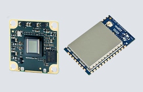


Analog Devices / Maxim Integrated MAX98380 Digital Input Class-D Amplifier
Analog Devices MAX98380 Digital Input Class-D Amplifier offers an integrated capacitive boost converter. The small, mono Class-D audio amplifier implements a triple charge pump-based boost converter that efficiently supplies up to 4.85W at 1% THD+N into an 8Ω load. The capacitive boost replaces the large and expensive inductor needed for an inductive boost with smaller, lower-profile capacitors, decreasing the total PCB solution.
The power supply voltage changes due to declining battery life, and an on-chip limiter (DHT) automatically optimizes the headroom available to the Class-D amplifier to maintain consistent distortion and listening levels. Thermal-foldback protection confirms robust behavior when the thermal limits of the MAX98380 are reached. When enabled, it automatically reduces the output power when the temperature exceeds a user-specified threshold, allowing for uninterrupted music playback even at high ambient temperatures. Traditional thermal protection is also available in addition to robust overcurrent protection.
The MAX98380 delivers a PCM interface for audio data and a standard I2C interface for control data communication. The PCM interface supports audio playback employing I2S, left-justified, and TDM audio data formats. A unique clocking structure eliminates requiring an external master clock for PCM communication. This structure reduces EMI, possible board coupling issues, and the size and pin count. Active emissions-limiting and edge-rate-limiting circuitry significantly mitigate EMI. A filterless spread-spectrum modulation scheme eliminates the demand for output filtering found in traditional Class-D devices and decreases the component count of the solution.
The ADI MAX98380 Amplifier is housed in a 0.35mm pitch 24-bump wafer-level package (WLP) and is specified over the extended temperature range of -40°C to +85°C.
Features
- Integrated capacitive boost converter - no bulky inductors
- 3.6W output power into 6Q at VBAT = 3.7V
- 10mW total quiescent power
- 3ms turn-on time
- 80% efficiency (1.0W into RL = 8Q, VBAT = 3.7V)
- 19.8µVRMS speaker mode output noise
- 16.5µVRMS receiver mode output noise
- Low 0.005% THD+N at 1kHz
- No MCLK required
- Sample rates of 8kHz to 192kHz
- Sophisticated edge rate control enables filterless
- Supports left, right, or (left/2 + right/2) output in I2S and left-justified modes
- Class-D outputs
- Low RF susceptibility rejects TDMA noise from GSM radios
- Class-D switching frequency trimmed to 10% for better EMI planning
- Extensive click-and-pop reduction circuitry
- Dynamic Headroom Tracking (DHT)
- Robust short-circuit and thermal protection available in space-saving package of 1.468mm x 2.138mm, 24-bump WLP (0.35mm pitch)
Applications
- Smartphones
- Smart speakers
- loT devices
- Tablets
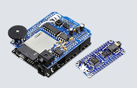
Associated Eval System

Analog Devices / Maxim Integrated MAX98380EVSYS Evaluation System
Thoroughly tested & assembled, designed to demonstrate the MAX98380 boosted Class-D audio amplifier.
Simplified Block Diagram
