


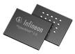
Infineon Technologies S27KS064x & S27KL064x HYPERRAM™ 2.0 Memory
Infineon Technologies S27KS064x and S27KL064x HYPERRAM™ 2.0 Memory are high-speed, low-pin-count DRAMs for high-performance embedded systems requiring expansion memory. These devices offer HYPERBUS™ and Octal SPI interfaces that draw upon the legacy features of both parallel and serial interface memories. These DRAMs operate at a voltage range of 1.8V to 3V and offer a bandwidth of up to 400MBps throughput. This makes HYPERRAM™ 2.0 the ideal expansion memory for controllers with limited onboard RAM. The HYPERRAM™ 2.0, when used as scratch-pad memory, allows the read and write operations to enable fast delivery of high-resolution graphics. Typical applications include automotive instrument clusters, industrial Human Machine Interface (HMI), industrial machine vision, and display systems for consumer electronics.
The Infineon Technologies S27KS064x and S27KL064x HYPERRAM™ 2.0 DRAMs are offered in a fortified Ball Grid Array (BGA) package.
Features
- Technology: 38nm DRAM
- HYPERBUS interface
- 8V to 3.0V interface support
- Single-ended clock (CK) - 11 bus signals
- Optional differential clock (CK, CK#) - 12 bus signals
- Chip Select (CS#)
- 8-bit data bus (DQ[7:0])
- Hardware reset (RESET#)
- Bidirectional Read-Write Data Strobe (RWDS)
- Output at the start of all transactions to indicate refresh latency
- Output during reading transactions as Read Data Strobe
- Input during write transactions as Write Data Mask
- Optional DDR Center-Aligned Read Strobe (DCARS)
- During read transactions, RWDS is offset by a second clock, phase-shifted from CK
- The Phase Shifted Clock is used to move the RWDS transition edge within the read data eye
- 200MHz maximum clock rate
- DDR - transfers data on both edges of the clock
- Data throughput up to 400MBps (3200Mbps)
- Configurable burst characteristics, linear burst
- Wrapped burst lengths
- 16 bytes (eight clocks)
- 32 bytes (16 clocks)
- 64 bytes (32 clocks)
- 128 bytes (64 clocks)
- Hybrid option - one wrapped burst followed by linear burst
- Configurable output drive strength
- Power modes
- Hybrid Sleep Mode
- Deep Power Down
- Array refresh
- Partial Memory Array (1/8, 1/4, 1/2)
- Full
- Operating temperature range
- Industrial (I): -40°C to +85°C
- Industrial Plus (V): -40°C to +105°C
- Automotive, AEC-Q100 Grade 3: -40°C to +85°C
- Automotive, AEC-Q100 Grade 2: -40°C to +105°C
- 6.0mm x 8.0mm x 1.0mm FBGA24 package
Applications
- Automotive instrument clusters
- Display systems for consumer electronics
- Consumer and industrial HMI
- Industrial machine vision
Videos
Logical Block Diagram

Related Products
Infineon Technologies S80KS2562 & S80KS2563 256Mb HYPERRAM™ 2.0 Memory
High-speed, low-pin-count, low-power self-refresh DRAM with a HyperBUS or Octal xSPI interface.
Publicado: 2020-02-24
| Actualizado: 2024-09-27