


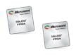
Microchip Technology IGLOO Nano Low Power Flash FPGAs
Microchip IGLOO Nano Low Power Flash FPGAs offer a single-chip solution, re-programmability, advanced features, and small footprint packages. These FPGAs incorporate Flash*Freeze technology that enables entering and exiting an ultra-low power mode by consuming nano power while retaining SRAM and registering data. This technology also simplifies power management through I/O and clock management with rapid recovery to an operation mode. The IGLOO nano-devices also incorporate non-volatile flash technology that instantly brings the secure, low-power, and single-chip solution. These features enable designers to create high-density systems using existing ASIC or FPGA design flows and tools. The IGLOO nano FPGAs offer 1kb of on-chip, reprogrammable, non-volatile FlashROM storage and clock conditioning circuitry based on an integrated Phase-Locked Loop (PLL). These Flash FPGAs are ideally used in consumer, industrial, communications, computing, networking, and avionics applications.
Features
- Low power:
- Nano power consumption - industry's lowest power
- 1.2V to 1.5V core voltage support for low power
- Supports single-voltage system operation
- Low-power active FPGA operation
- Flash*Freeze technology enables ultra-low power
- Consumption while maintaining FPGA content
- Easy entry to / exit from ultra-low power Flash*Freeze mode
- High capacity:
- 10,000 to 250,000 system gates
- Up to 36Kb of true dual-port SRAM
- Up to 71 users I/Os
- Reprogrammable flash technology:
- 130nm, 7-layer metal, flash-based CMOS process
- Instant on level 0 support
- Single-chip solution
- Retains programmed design when powered off
- 250MHz for 1.5V systems and 160MHz for 1.2V systems
- High-performance routing hierarchy:
- Segmented, hierarchical routing, and clock structure
- In-System Programming (ISP) and security:
- ISP using on-chip 128-Bit Advanced Encryption Standard (AES) Decryption via JTAG (IEEE 1532-compliant)
- FlashLock® designed to secure FPGA contents
- 1.2V programming
- Embedded Memory:
- 1Kb of FlashROM user non-volatile memory
- SRAMs and FIFOs with variable-aspect-ratio 4608-Bit RAM blocks (×1, ×2, ×4, ×9, and ×18 organizations)
- True dual-port SRAM (except ×18 organization)
- Advanced I/O:
- 1.2V, 1.5V, 1.8V, 2.5V, and 3.3V mixed-voltage operation
- Wide range power supply voltage support per JESD8-B, allowing I/Os to operate from 2.7V to 3.6V
- Wide range power supply voltage support per JESD8-12, allowing I/Os to operate from 1.14V to 1.575V
- Bank-selectable I/O voltages up to 4 banks per chip
- Single-ended I/O standards:
- LVTTL, LVCMOS 3.3V/2.5V/1.8V/1.5V/1.2V
- I/O registers on input, output, and enable paths
- Hot-swappable and cold-sparing I/Os
- Programmable output slew rate and drive strength
- Weak pull-up/pull-down
- IEEE 1149.1 (JTAG) Boundary-Scan test
- Pin-compatible packages across the IGLOO family
- Clock Conditioning Circuit (CCC) and PLL:
- Up to Six CCC blocks and one with an integrated PLL
- Configurable phase-shift, multiply/divide, delay capabilities, and external feedback
- 1.5MHz to 250MHz wide input frequency range
Applications
- Consumer
- Network
- Computing
- Avionics
- Communications
Additional Resource
Related Products

Microchip Technology ProASIC3 Flash FPGAs
Offer higher performance, greater density, and features for demanding high-volume applications.
Microchip Technology IGLOO Low Power Flash FPGAs
Offer a single-chip solution, small footprint packages, re-programmability, and advanced features.

Microchip Technology M1A3P600 ProASIC3 Flash FPGAs
Offer high-performance, density, and features for the demanding high-volume applications.
Publicado: 2019-06-19
| Actualizado: 2023-06-02