


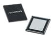
Renesas Electronics 5G Radio Synchronizer & RF Sampling Clock Solution
Renesas Electronics 5G Radio Synchronizer and RF Sampling Clocks Solution product portfolio has expanded to include three devices for RF sampling clock conditioning frequency/phase management and radio synchronization.
The 8V19N850 is a monolithic integration of a digital clock front-end for network synchronization (Synchronous Ethernet, IEEE 1588) with an RF sampling generator. The 8V19N850 offers an integrated 5G radio synchronization solution with full IEEE 1588, EEC, and JESD204B/C compliance. The device contains a complete set of radio synchronization features, with low phase noise, high frequency, and low spurious RF sampling clock.
The 8V19N880and 8V19N882 generate multiple, synchronized, low phase noise (80fs RMS) and low spurious clock signals for DAC/ADC circuits (standalone and integrated radio transceivers), ensuring the best possible (A/D, D/A) conversion parameters. A low phase noise clock signal improves system characteristics in radio equipment, such as signal to noise ratio (SNR), Error vector magnitude (EVM), and minimized blocker signals. As a result, the low phase noise supports better reception and transmit characteristics and reducing radio signal interference.
All three devices enable the best possible ENOB (effective number of bits) performance for data converters in data sampling applications. The Renesas 5G Radio Synchronizer and RF Sampling Clocks offer improved phase noise versus existing solutions, added functional flexibility, and enable customers to use a 1.8V power supply (8V19N880 and 8V19N882). The 8V19N882 (QFN package) is a derivative of the 8V19N880 (BGA package) with less I/O, and it supports a more extensive range of supply voltages than 8V19N880.
Applications
- 8V19N880, 8V19N882:
- Wireless infrastructure/4G and 5G, AAS, <6GHz and >6GHz carrier (mmWave), beamforming
- Satellite receiver, radar, tactical radio
- High-speed optical networking >100Gbit/s modules
- High-performance data sampling such as instrumentation applications
- 8V19N850:
- Wireless infrastructure/5G radios and small cell radios
Associated Products
Renesas Electronics 8V19N850 RF Sampling Clock Generator
A single component solution that integrates up to 4 discrete components (sync, 2x JA, VCXO).
Renesas Electronics 8V19N882 RF Clock Generator & Jitter Attenuator
A clock solution for conditioning and management of wireless base station radio equipment boards.
4G vs 5G Comparison
