


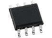
Renesas Electronics 9FGL0x Clock Generators
9FGL0x Clock Generators are 3.3V PCIe Gen1-5 generators with 2, 4, and 8 100MHz PCIe output pairs. These buffers come with 2, 4, and 8 100MHz PCIe output versions. The 9FGL0x generators feature integrated terminations for 100Ω and 85Ω systems, 112mW to 206mW typical power consumption (at 3.3V), and 25MHz input frequency. These generators also feature pin-selectable SRnS 0%, CC 0%, CC/SRIS 0.5% spread, and SMBus-selectable CC/SRIS -0.25% spread. Typical applications include nVME storage, networking, accelerators, industrial control, and servers/high-performance computing.
Features
- 2, 4, or 8 100MHz PCIe output pairs
- One 3.3V LVCMOS REF output with Wake-OnLAN (WOL) support
- Integrated terminations for 100Ω and 85Ω systems save 4 resistors per output
- 112mW to 206mW typical power consumption (at 3.3V)
- VDDIO rail allows 35% power savings at optional 1.05V (9FGL06 and 9FGL08 only)
- Devices contain default configuration; SMBus not required
- Contact the factory for custom default configurations
- SMBus-selectable features allow optimization to customer requirements:
- Input polarity and pull-up/pull-downs
- Output slew rate and amplitude
- Output impedance (85Ω or 100Ω) for each output
- OE# pins support PCIe CLKREQ# function
- Pin-selectable SRnS 0%, CC 0%, and CC/SRIS 0.5% spread
- SMBus-selectable CC/SRIS -0.25% spread
- Clean switching between the CC/SRIS spread settings
- DIF outputs are blocked until PLL is locked; clean system start-up
- 2 selectable SMBus addresses
- Space-saving packages:
- 4mm × 4mm 24-VFQFPN (9FGL02x1D)
- 5mm × 5mm 32-VFQFPN (9FGL04x1D)
- 5mm × 5mm 40-VFQFPN (9FGL06x1D)
- 6mm × 6mm 48-VFQFPN (9FGL08x1D)
Specifications
- 90fs RMS typical jitter (PCIe Gen5 CC)
- <50ps cycle-to-cycle jitter on differential outputs
- <50ps output-to-output skew on differential outputs
- ±0ppm synthesis error on differential outputs
- 25MHz input frequency
Applications
- Servers/high-performance computing
- nVME storage
- Networking
- Accelerators
- Industrial control
Block Diagram

Additional Resources
- AN-805 – Recommended Ferrite Beads
- Application Relevance of Clock Jitter
- Application Note-Cascading PLLs
- Driving LVPECL, LVDS, CML and SSTL Logic with IDT’s “Universal” Low-Power HCSL Outputs
- Low-Power HCSL vs. Traditional HCSL
- PCI Express Reference Clock Requirements
- Thermal Considerations in Package Design and Selection
- Jitter Specifications for Timing Signals
- RMS Phase Jitter
- Differential Input with VCMR being VIH Referenced
- Differential Input to Accept Single-Ended Levels
- Understanding Jitter Units
- Crystal - Measuring Oscillator Negative Resistance
Related Products
Renesas Electronics Soluciones de circuitos integrados (IC) de temporización de reloj
Soluciones de temporización de reloj para conexión de red y comunicaciones, consumidores y aplicaciones informáticas.
Renesas Electronics 9DBL0x Fanout Buffers
Low-power, high-performance, and support PCIe Gen1 through Gen5.

Renesas Electronics RC190x Fanout Buffers
Ultra-high-performance fanout buffers support PCIe Gen5 and PCIe Gen6.

Renesas Electronics RC192x Clock Muxes
Ultra-high-performance clock muxes supporting PCIe Gen5/Gen6 with Loss-Of-Signal (LOS).

Renesas Electronics FEMTOCLOCK3 Clock Generators/Synthesizers
Low-cost, high-quality, low-jitter clock signals with less than 0.5ps of RMS phase noise.

Renesas Electronics RC22112A FemtoClock™ Clock Generator
Features PCIe Gen 1-6 CC, fully integrated, low-power, and high-performance clock generator.

Renesas Electronics RC32508A Evaluation Board
Designed to evaluate the RC32508A jitter attenuator and clock generator.
| N.º de artículo | Número de salidas | Voltaje de alimentación - Máx. | Voltaje de alimentación - Mín. | Ciclo de tarea - Máximo | Sensibles a la humedad | Corriente de suministro operativa | Temperatura de trabajo máxima | Temperatura de trabajo mínima | Hoja de datos |
|---|---|---|---|---|---|---|---|---|---|
| 9FGL0841DKILFT | 8 Output | 3.465 V | 3.135 V | 55 % | Yes | 23 mA | + 85 C | - 40 C |  |
| 9FGL0241DKILF | 2 Output | 3.465 V | 3.135 V | 55 % | 23 mA | + 85 C | - 40 C | |
|
| 9FGL0851DKILFT | 8 Output | 3.465 V | 3.135 V | 55 % | Yes | 23 mA | + 85 C | - 40 C | |
| 9FGL0451DKILFT | 4 Output | 3.465 V | 3.135 V | 55 % | Yes | 23 mA | + 85 C | - 40 C | |