




Texas Instruments LMKDB12xx LP-HCSL Clock Multiplexers

Texas Instruments LMKDB12xx LP-HCSL Clock Multiplexers are extremely low-jitter clock muxes for PCIe clocking applications from PCIe Gen 1 to PCIe Gen 7. The series includes the LMKDB1202, LMKDB1204, and LMKDB1208 devices and supports common clock and independent-reference PCIe architectures, with input clocks that use or do not use spread-spectrum clocking.
The TI LMKDB12xx multiplexers are DB2000QL compliant and provide built-in features for robust clock distribution, including fail-safe inputs, flexible power-up sequencing, individual output enable, automatic output disable, and loss-of-signal input detection. The LMKDB12xx LP-HCSL Clock Multiplexers also include an SBI sideband interface for high-speed control of output enable/disable.
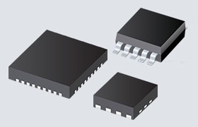
The clock multiplexers are excellent for high-performance computing, server motherboards, NICs, SmartNICs, and hardware accelerators. The LMKDB12xx supports 1.8V and 3.3V power rails and is available in 20-pin, 28-pin, and 48-pin VQFN package options.
Features
- LP-HCSL clock mux support for PCIe Gen 1 to Gen 7 systems
- DB2000QL compliance across all devices
- Low additive jitter performance
- 31fs maximum RMS additive jitter from 12kHz to 20MHz at 156.25MHz
- 13fs maximum additive jitter for PCIe Gen 4
- 5fs maximum additive jitter for PCIe Gen 5
- 3fs maximum additive jitter for PCIe Gen 6
- 2.1fs maximum additive jitter for PCIe Gen 7
- Support for common clock and independent reference PCIe architectures
- Input clock operation with or without spread-spectrum clocking
- Fail-safe input and flexible power-up sequence support
- Automatic output disable, and individual output enable features
- SBI sideband interface for high-speed output enable or disable control
- LOS input detection for loss-of-signal monitoring
Applications
- High-performance computing
- Server motherboard
- NIC/SmartNIC
- Hardware accelerator
Specifications
- Package options
- LMKDB1208 RSL 48-pin VQFN package, 6mm x 6mm
- LMKDB1204 REX 28-pin VQFN package, 4mm x 4mm
- LMKDB1202 REY 20-pin VQFN package, 3mm x 3mm
- Output impedance options of 85Ω or 100Ω
- Power supply support of 1.8V or 3.3V ±10%
- Ambient temperature range of -40°C to +105°C
Eval Modules

Texas Instruments LMKDB1204EVM Evaluation Module (EVM)
Designed to evaluate the LMKDB1204 LP-HCSL buffer that supports PCIe Gen 1 to Gen 6.

Texas Instruments LMKDB1x02EVM Evaluation Modules
Designed to quickly demonstrate the LMKDB1x02 LP-HCSL buffer, which supports PCIe Gen 1 to 6.
Associated Buffers

Texas Instruments LMKDB1 Ultra-Low Jitter Clock Buffers
LP-HCSL buffers and MUX that support PCIe Gen 1 to Gen 6 that are DB2000QL compliant.
Additional Resources
Typical Application
