


Texas Instruments MSPM0Lx22x/MSPM0Lx22x-Q1 Mixed-Signal MCUs

Texas Instruments MSPM0Lx22x/MSPM0Lx22x-Q1 Mixed-Signal Microcontrollers (MCUs) are part of the highly integrated, ultra-low-power 32-bit MSPM0 MCU family based on the Arm® Cortex®-M0+ 32-bit core platform, operating at up to 32MHz. These MCUs offer a blend of cost optimization and design flexibility for applications requiring 128KB to 256KB of flash memory in small packages (down to 4mm x 4mm) or high pin count packages (up to 80 pins). These devices include a VBAT backup island, an optional segmented LCD controller (on MSPM0L222x), cybersecurity enablers, and high-performance integrated analog, and provide excellent low-power performance across the operating temperature range.
Texas Instruments MSPM0Lx22x/MSPM0Lx22x-Q1 Mixed-Signal MCUs provide up to 256KB of embedded Flash program memory with built-in error correction code (ECC) and up to 32KB of SRAM with ECC and parity protection. An ultra-low-power segmented LCD controller (on MSPM0L2228 / MSPM0L2228-Q1 and MSPM0L2227 / MSPM0L2227-Q1 devices) supports driving LCD glass with up to 59 pins in various mux and bias configurations, enabling cost-effective displays.
Flexible cybersecurity enablers can support secure boot, secure in-field firmware updates, IP protection (execute-only memory), key storage, and more. The cybersecurity architecture is Arm PSA Level 1 certified. A set of high-performance analog modules is provided, including a 12-bit 1.68Msps SAR ADC supporting up to 26 external channels. An analog comparator is provided to support low-power or low-latency monitoring of analog signals. An on-chip voltage reference (1.4V or 2.5V) can provide a stable reference voltage to the ADC and comparator. The MSPM0Lx22x-Q1 devices are AEC-Q100 qualified for automotive applications.
Features
- Core
- Arm 32-bit Cortex-M0+ CPU with memory protection unit, frequency up to 32MHz
- PSA-L1 Certified
- Operating characteristics
- -40°C up to 125°C extended temperature
- 1.62V to 3.6V wide supply voltage range
- Memories
- Up to 256KB of Flash memory with ECC- dual-bank with address swap and OTA updates
- 32KB of SRAM with ECC or parity
- 32B backup memory
- High-performance analog peripherals
- 12-bit 1.68Msps analog-to-digital converter (ADC), up to 26 external channels
- Configurable 1.4V or 2.5V internal shared voltage reference (VREF)
- Comparator (COMP) with 8-bit reference DAC
- Integrated temperature sensor
- User interface with an ultra-low power segmented LCD controller supporting up to 8×51 and 4×55 LCDs
- Optimized low-power modes
- RUN: 106µA/MHz (CoreMark)
- STOP: 54µA at 32kHz
- STANDBY 1.2µA (VDD), 1.1µA (VBAT) with 32kHz, LFXT, RTC, and SRAM and registers fully retained
- SHUTDOWN: 80nA (VDD), 1.1µA (VBAT) with 32kHz, LFXT, RTC, and I/O wake-up
- Intelligent digital peripherals
- 7-channel DMA controller
- 15-channel event fabric signaling system
- Six timers supporting up to 18 PWM outputs, all operational down to STANDBY mode
- One 16-bit advanced timer with deadband
- One 32-bit general-purpose timer
- Four 16-bit general-purpose timers
- Window-watchdog timer (WWDT)
- Independent watchdog timer (IWDT) residing on the VBAT island
- Communication interfaces
- Five UART modules, with two supporting LIN, IrDA, DALI, smart card, and Manchester
- Three I2C modules supporting SMBus/PMBus and wakeup from STOP mode, with two supporting up to FM+ (1Mbps)
- Two SPI modules supporting up to 16Mbps
- Clock system
- Internal 4MHz to 32MHz oscillator with up to ±1.2% accuracy (SYSOSC)
- Internal 32kHz oscillator (LFOSC) with ±3% accuracy
- External 4MHz to 32MHz crystal oscillator (HFXT)
- External 32kHz crystal oscillator (LFXT)
- External LF and HF digital clock inputs
- Digital clock output
- Data integrity and encryption
- AES accelerator with support for GCM/GMAC, CCM/CBC-MAC, CBC, CTR
- Secure Key storage for up to four AES keys
- Flexible firewalls for protecting code and data
- True random number generator (TRNG)
- Cyclic redundancy checker (CRC-16, CRC-32)
- VBAT island (auxiliary supply)
- Independent supply with dedicated VBAT pin
- Internal supercapacitor charger
- Real-time clock (RTC)
- Tamper detection with timestamp
- Independent watchdog timer (IWDT)
- Scratch Pad Memory (SPM)
- Flexible I/O features
- Up to 73 total GPIOs
- Up to five GPIOs supplied by VBAT pin
- Development support of 2-pin serial wire debug (SWD)
- Package options
- 80-pin LQFP
- 64-pin LQFP
- 48-pin LQFP, VQFN
- 32-pin VQFN
- 24-pin VQFN
- Family members
- MSPM0L2228: 256KB Flash, LCD
- MSPM0L2227: 128KB Flash, LCD
- MSPM0L1228: 256KB Flash
- MSPM0L1227: 128KB Flash
- Development kits and software
- LP-MSPM0L2228 LaunchPad™ development kit
- MSP Software Development Kit (SDK)
Applications
- Electric and hybrid vehicles (EVs and HEVs)
- Grid infrastructure
- Factory automation and control
- Appliances
- Medical and healthcare
- Test and measurement
Videos
Functional Block Diagram

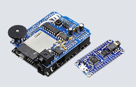
Development Tool

Texas Instruments C-GANG Low-Cost Gang Programmer
Gang programmer can program up to six targets at once & is compatible with the MSPM0/MSP430 devices.