


Texas Instruments TPS22810/TPS22810-Q1 Load Switches
Texas Instruments TPS22810/TPS22810-Q1 Load Switch is a single channel load switch with configurable rise time and with an integrated quick output discharge (QOD). The device features thermal shutdown to protect the load switch against high junction temperature. Because of this feature, the safe operating area of the device is inherently ensured. The TPS22810/Q1 contains an N-channel MOSFET that can operate over an input voltage range of 2.7V to 18V. The SOT23-5 package can support a maximum current of 2A while the WSON package can support a maximum current of 3A. The switch is controlled by an on and off input, which is capable of interfacing directly with low-voltage control signals. The TPS22810-Q1 devices are AEC-Q100 qualified for automotive applications.
Features
- Integrated single channel load switch
- –40°C to +105°C Ambient operating temperature
- SOT23-6 (DBV): 2A Maximum continuous current 1
- WSON (DRV): 3A Maximum continuous current 1
- 2.7V to 18V Input voltage range
- 20V Absolute maximum input voltage
- On-Resistance (RON)
- RON = 79mΩ (typical) at VIN = 12V
- Quiescent Current
- 62µA (typical) at VIN = 12V
- Shutdown Current
- 500nA (typical) at VIN = 12V
- Thermal shutdown
- Undervoltage Lock-Out (UVLO)
- Adjustable Quick Output Discharge (QOD)
- Configurable rise time With CT pin
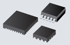
- SOT23-6 Package
- 2.9mm × 2.8mm, 0.95mm pitch
- 1.45mm Height (DBV)
- WSON Package
- 2mm × 2mm, 0.65mm Pitch
- 0.75mm Height (DRV)
- ESD Performance tested per JESD 22
- ±2kV HBM and ±1kV CDM
Applications
- HD TV
- Industrial systems
- Set top box
- Surveillance systems
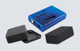
TPS22810EVM Evaluation Module
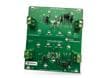
Texas Instruments TPS22810EVM Evaluation Module (EVM)
Fully assembled and tested circuit for evaluating the TPS22810 single channel load switch.
Datasheets
TPS22810 Block Diagram

Publicado: 2017-08-08
| Actualizado: 2022-04-01